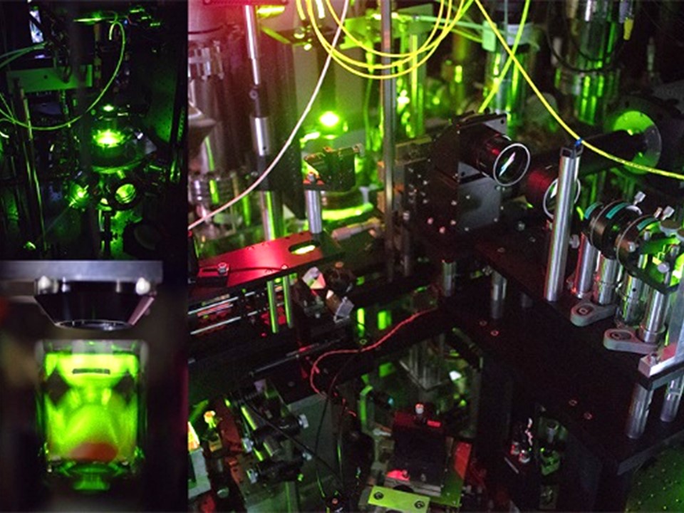
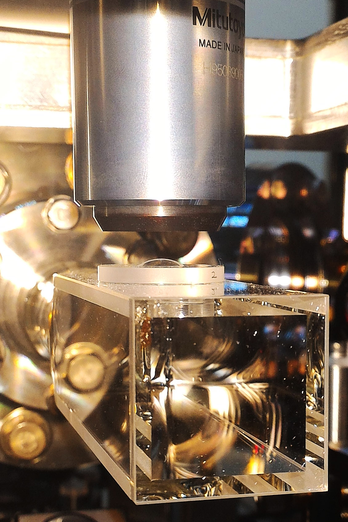
We are interested in condensed matter physics emerging in the cold atomic gas trapped in the periodic optical potential, i.e., an optical lattice. We have recently implemented a quantum gas microscope for Ytterbium atoms, by which we can monitor individual atoms with site-resolution. The photograph shows our experimental apparatus.
The optical standing wave with its frequency far detuned concerning the atomic transition works as a periodic potential for atoms which is called an optical lattice. In solid crystals, electrons are trapped in the lattice made by regularly arranged ions. Loading quantum degenerate atomic gas in the optical lattice, we can perform various types of quantum simulations, where the ion lattice and electrons are replaced with the optical lattice and cold atoms, respectively.
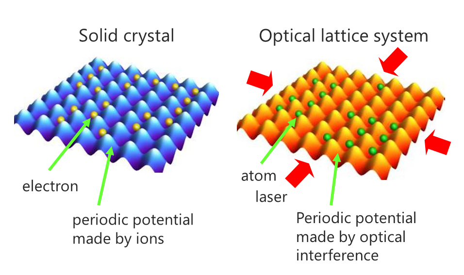
Since the optical interference makes the optical lattice, unwanted defects do not exist. Laser cooling procedure can select specific atomic species (even isotope), and the system thus does not have impurities. By cutting off the laser, atoms can freely diffuse in the vacuum, and atom density profile provides us with information of initial momentum distribution. By changing the number, crossing angle and wavelength of the laser beams, we can create not only a simple tetragonal lattice but also a honeycomb lattice, quasicrystal and so on. The period of the optical lattice is two orders of magnitude longer than that of the solid crystal, and the mass of the atom is three to five orders of magnitude larger than that of the electron. Therefore tunneling rate is extremely slow in the optical lattice (typically ms order), which enables us to trace the system dynamics in real time. The optical lattice system is a quantum many-body system with large degrees of freedom which is ideal for approaching the microscopic understanding of various physical phenomena emerging in solids.
Here is one example. The transition temperature of the cuprate superconductor has rapidly risen since its discovery in 1986, and industrial applications are being examined in various forms as well. Conventional superconductors can be explained by the BCS theory that Cooper pairs are created by the interaction between electrons and lattices. However, in the case of cuprates superconductor, the complete understanding has not yet been obtained about the mechanism of electron pair creation. Typical phase diagram for a cuprates superconductor has been experimentally investigated. As shown below, as the temperature becomes less than the Neel temperature, an antiferromagnetic phase appears, and as the hole concentration increases, d-wave superconductivity emerges.
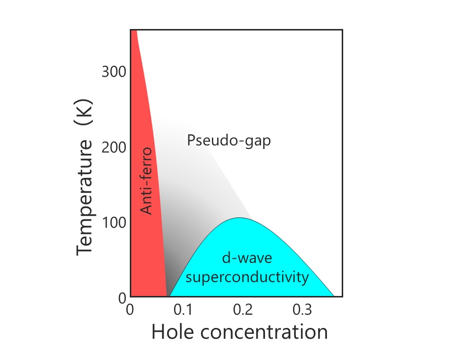
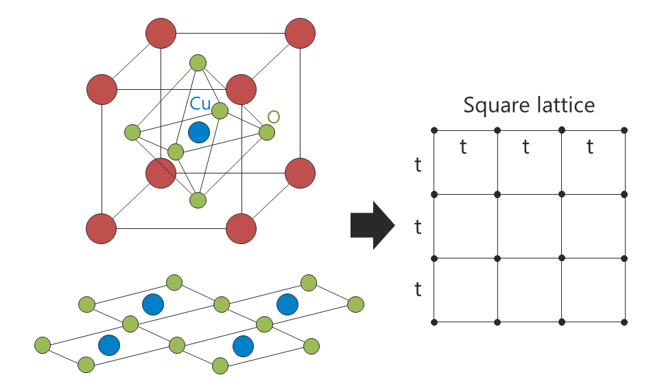
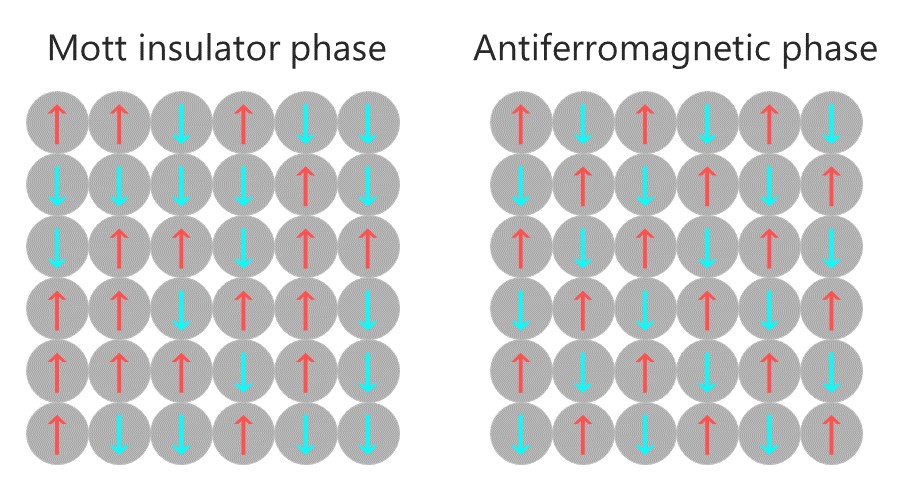
The cuprate superconductor has a square lattice structure composed of copper and oxygen atoms. At temperatures higher than the Neel temperature, Mott insulator phase appears in which the spin direction is disordered, and one electron occupies each site. When the system is cooled below the Neel temperature, the spin is ordered by the superexchange interaction, and the antiferromagnetic phase appears. Then as the hole concentration is increased, an electron pair is created, and a superconducting phase appears. Through experiments using high-quality samples, it is elucidated that the symmetry of the order parameter is d-wave. These facts predict that electron pairs are created through antiferromagnetic fluctuations of spins, but the details have not yet clarified. Also, looking at the phase diagram, we notice that there is a region called a pseudogap in which a gap-like structure appears in the electron excitation spectrum despite a normal conducting phase. Although this pseudogap is considered to be deeply related to the mechanism of high-temperature superconductivity, its microscopic understanding has not yet been obtained. Introducing Fermi degenerate gas of atoms into the optical lattice and generating the Mott insulator phase, antiferromagnetic phase, d-wave superconducting phase, and even pseudogap, we will be able to approach the microscopic understanding of the physics of high-temperature superconductivity.
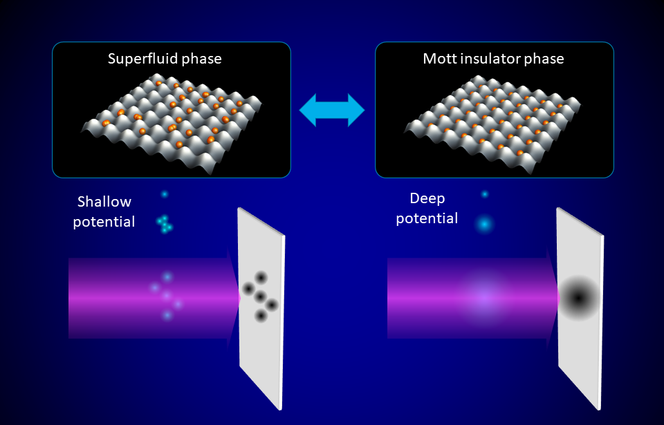
An absorption imaging has been widely utilized to observe quantum phases that appear in the optical lattice. Cutting off the laser beams generating the optical lattice, let the atoms diffuse in the vacuum. After irradiating the atom cloud with a resonant probe beam, the intensity profile of the probe is monitored with a CCD camera and the atom density distribution is evaluated, from which one can estimate the quantum states of atoms in the optical lattice. As an example, let's consider the case where Bose-Einstein condensate is loaded into the optical lattice. When the depth of the optical lattice is sufficiently shallow, a superfluid phase appears. Since the atoms frequently tunnel between the sites and non-diagonal long-range order is maintained, the absorption imaging can obtain clear interference fringes. On the other hand, when the optical lattice is sufficiently deep, tunneling is suppressed, and the onsite interaction becomes dominant. Under such a condition, atoms try to avoid entering the same site and Mott insulator phase where one atom occupies each site emerges. Because the number of atoms in each site is fixed, interference fringes disappear.
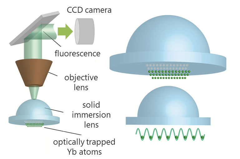
Absorption imaging is an excellent technique that utilizes the fact that the density profile of sufficiently diffused atom cloud reflects the momentum distribution. However, it is difficult to check whether each site is occupied by one atom or not. Recently, a quantum gas microscope technique has appeared, and direct observation of the occupation of each site became possible. We have also succeeded in realizing a quantum gas microscope for a lanthanoid atom called ytterbium (Yb). We prepared a two-dimensional optical lattice about 1 micron below the surface of a hemispherical lens called a solid immersion lens. The solid immersion lens can increase the resolution of the optical microscope by a factor of its refractive index. The schematic diagram of our quantum gas microscope and a photograph of the apparatus are shown below.
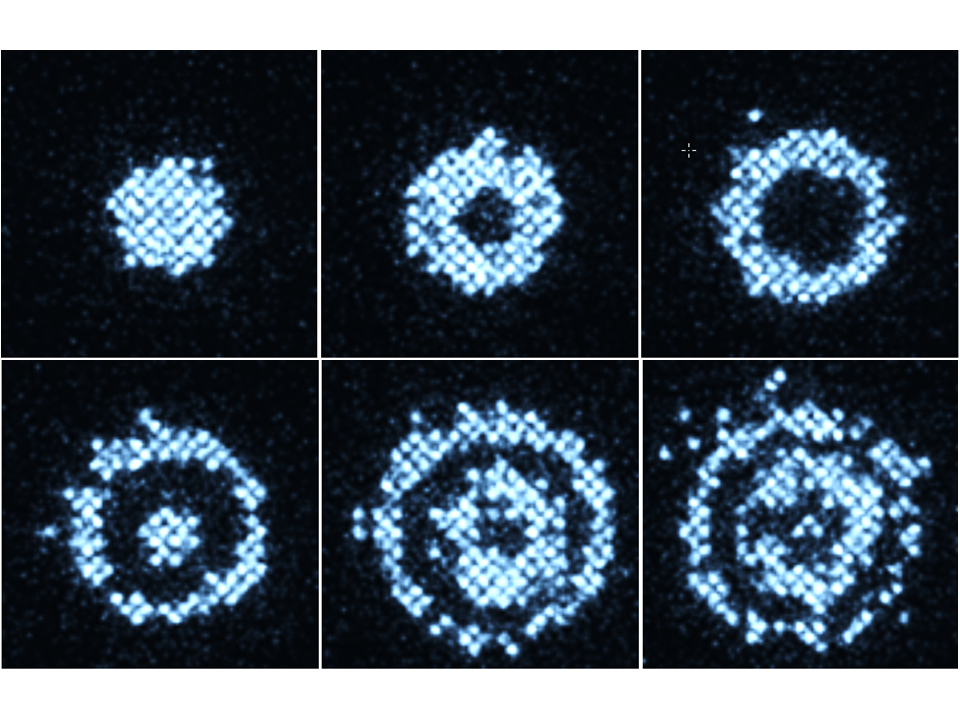
When we want to observe the atoms in the optical lattice, we irradiate the system with excitation light and detect the atom fluorescence with an EM-CCD camera. An example of a fluorescent image of Yb atoms in the optical lattice obtained by our quantum gas microscope is shown below.
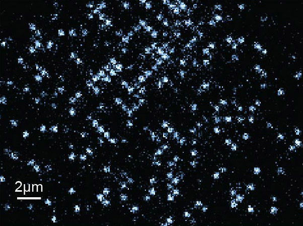
Yb has five bosonic and two fermionic isotopes. The system in which the fermionic isotope is loaded into the 2D optical lattice resembles the structure of the cuprates superconductor described earlier. Mott insulator phase, antiferromagnetic phase, and other characteristic quantum phases can be observed directly with this quantum gas microscope. The figure below shows the Mott insulator phase observed by our quantum gas microscope, where the Mott insulator was generated by loading bosonic isotope to the 2D optical lattice. In this experiment, we excluded an even number of atoms from the site in advance by using a photo-association technique which converts two atoms into one molecule. As the total number of atoms lattice increases, the number of atoms in the site increases stepwise from the outside. Such a structure is called a Mott shell. We are aiming to approach a microscopic understanding of high-temperature superconductivity by using the quantum gas microscope.